
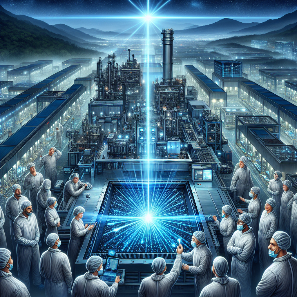
A Flash of Light in a Silent Factory
It’s sometime past midnight, but the factory floor hums with quiet urgency. At the heart of the world’s most advanced chip foundry, a blinding pulse explodes in a sealed, silent vacuum chamber—a speck of tin, vaporized, flares brighter than the sun’s surface for a millisecond. Somewhere on the other side of reinforced glass, an engineer’s tired eyes widen in awe. This, they know, is the beat that powers every new phone, every AI breakthrough, and the digital future itself.
Tonight, in this nearly sterile place, the latest chapter of microchip history is being etched—literally—by light that Earth never sees.
Beyond the Edge: The Race Past EUV
For decades, making microchips smaller, faster, and more efficient has been a race against the laws of physics. Traditional methods used ultraviolet (UV) light to “print” intricate circuits onto silicon wafers, shrinking the wiring with every new generation[1][3]. But the industry hit a wall. Smaller patterns meant needing shorter light waves—waves so tiny, engineers began chasing extreme ultraviolet (EUV) light, 13.5 nanometers short, to etch lines just a few atoms wide[2][4].
Even EUV seemed impossible. To make this radiation, you fire a high-powered CO₂ laser at a droplet of tin—turning it into plasma heated to 220,000 degrees Celsius, almost 40 times hotter than the Sun’s surface. That plasma emits a flash of EUV light, captured and bounced by ultra-smooth mirrors, whose surfaces must be among the most flawless on Earth[1][3][4].
It was science fiction. Then, suddenly, it wasn’t.
Anatomy of a Breakthrough
Here’s where the new wave begins: a team of researchers claims they’ve pushed beyond the longstanding EUV limits, crafting circuitry at scales traditional methods couldn’t touch[2]. Details remain sparse—trade secrets, NDAs, and industry spies keep specifics in the dark—but they hint at manipulating patterns smaller than previously possible, perhaps with hybrid light sources or novel materials that capture and direct photons more precisely than ever.
Think of the system as the ultimate cosmic slide projector. A detailed blueprint (the “mask”) is illuminated by EUV flashes; the pattern is shrunk down and etched into silicon using a chemical “photoresist,” a substance so delicate it can only exist in vacuum—and only for moments at a time. Each pulse must be perfectly timed. Any glitch and the entire process collapses, taking millions of dollars’ worth of silicon with it[1][4].
Why It Matters: The Human Story
“Most people have no idea that the magic in their phone’s pocket depends on light from vaporized tin,” says Dr. Lin Ma, a leading semiconductor physicist. “It’s like painting on grains of sand—with lightning.”
Consider a fictional but relatable story: Nadia, a young engineer in Taiwan, wakes before dawn so her toddler can video-call their grandmother in the U.S. The live, high-def chat works flawlessly, powered by chips probably made using these next-gen techniques. For her family—and billions globally—these leaps aren’t just about profits. They’re about connection, education, accessibility.
Governments, Giants, and the Ripple Effect
No innovation this fundamental happens in a vacuum. When news broke of the breakthrough, governments and chip giants scrambled. In Washington, intelligence officials warned that next-gen chip tech could shift the world’s balance of power, fueling “the next quantum leap in AI, defense, and critical infrastructure,” according to a leaked government memo.
Analyst Mark Witherspoon notes, “If you control sub-2nm manufacturing, you don’t just lead tech—you lead economies, militaries, even geopolitics.” Already, industrial alliances are forming, with immense subsidies flowing toward any nation with a shot at mastering the post-EUV era.
Could It Happen to You? The Personal Scenario
Imagine a future where a new wearable device could monitor your health at a cellular level, catching diseases before you ever feel sick. Or a city where autonomous electric taxis use chips a hundred times more powerful than today—safer, faster, greener. But it also means a world where every digital move, every byte of our lives, is etched onto tin-plasma-washed silicon, in unseen factories half a world away.
Response and the Road Ahead
The industry reacted with a mix of awe and anxiety. Some celebrate a “new Moore’s Law”; others warn of cybersecurity threats and monopoly risks, as only a handful of firms worldwide control these cosmic foundries.
Still, the question burns: How much smaller can we go? Are there limits the universe simply won’t let us cross—or will human ingenuity, once again, redefine what’s possible?
What’s Next: The Frontier Isn’t Closed
As chip engineers stare, bleary-eyed, at the first new silicon wafers rolling out of their machines, one thing is clear: the race isn’t finished. This is just a step—an audacious leap—into even stranger, less-charted territory.
Are we witnessing the dawn of an era where matter, light, and code fuse into one—and if so, do we really understand the forces we’re about to unleash?
FAQ
-
What is post-EUV microchip manufacturing?
It’s the next step after extreme ultraviolet lithography, using methods and materials that allow for even smaller, faster, more energy-efficient chips than EUV ever could. -
Why is tin plasma used in chipmaking?
Tiny droplets of tin are vaporized by lasers to create plasma, emitting the ultra-short wavelength light necessary for the smallest chip features[1][2][4]. -
How does EUV lithography differ from traditional photolithography?
Traditional methods use longer-wavelength light, limiting how small chips can be. EUV uses ultra-short 13.5nm light, letting engineers etch much finer patterns[1][3][4]. -
Who leads in advanced chip manufacturing now?
Companies like ASML supply most EUV machines, with powerhouses in Taiwan, South Korea, and Japan rapidly pushing boundaries[2][5]. -
What could post-EUV chips enable?
From longer battery life to exponentially smarter AI, chips etched with these methods could underpin future supercomputers, medical devices, and quantum tech.